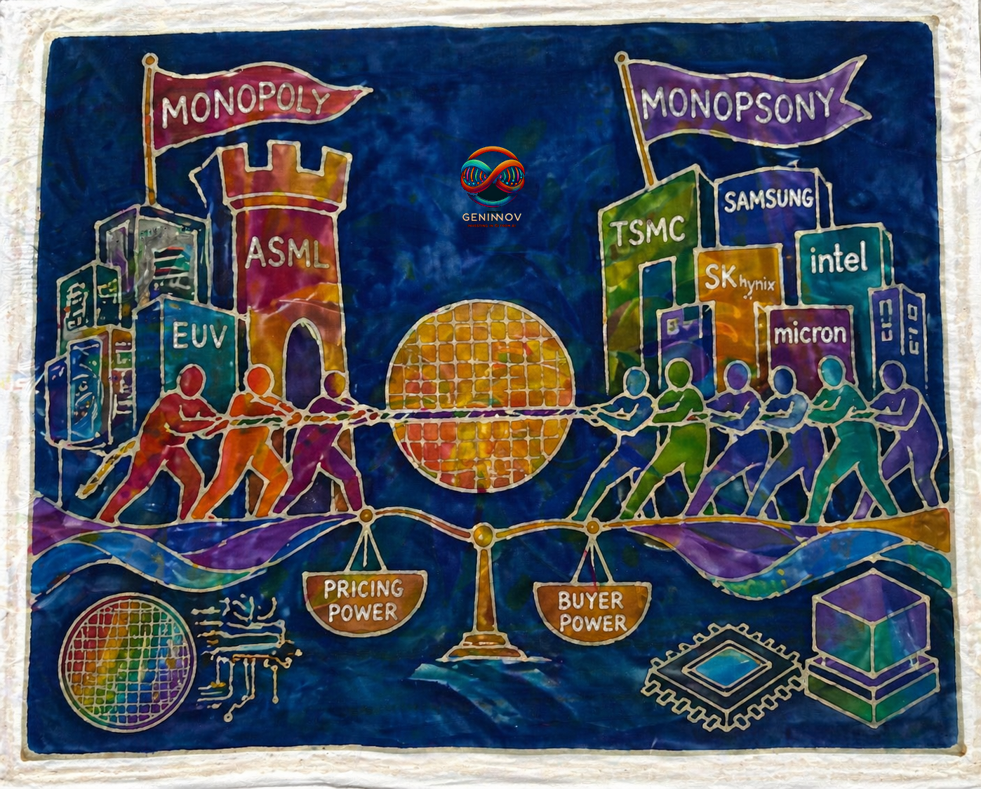
Some seemingly regular events are so massive in their implications across various domains that they deserve their own write-up. TSMC’s highly unusual public complaint of ASML’s latest EUV pricing falls in that category. Not only because the “very very expensive” complainer is relentless in utilizing its own pricing power, but also because it is not usual for these institutions to wash their dirty linen in public. We had discussed the near-monopsony and near-monopoly clash one sees in the TSMC and ASML battle first in 2024. Time to refresh in more detail as we traverse through Musk’s Terafab, Japan’s Rapidus, Samsung’s strike, and a few other topics, while first discussing whether ASML’s famed equipments are sufficient when one is thinking about a fab, aka whether a fab can be built by anyone with enough cash, and then whether they are necessary.
Part One: the Sufficient Question
The premise sounds rhetorical, almost juvenile. Of course a fab is more than an ASML machine. But the version of this question worth asking is sharper. Every semiconductor fab in the world is a collection of equipment whose suppliers are well-known and, China aside, accessible to any major economy or tech oligarch with the cash to pay. So can someone with enough will and enough budget build a leading-edge fab from a standing start?
The Catalog is Open. The Barrier is Elsewhere.
Walk through what a leading-edge capital expenditure actually buys. You get EUV scanners from ASML. You get deposition and etch tools from Lam Research, Applied Materials, and Tokyo Electron. You fold in metrology and materials from KLA, Shin-Etsu, Lasertec, BESI, and Teradyne. The tools are astronomically expensive, but the catalog is wide open.
Yet, this open catalog raises a glaring paradox: Why would TSMC, currently benefiting from an unprecedented global supply crunch, use plans to defer its latest fab development as a negotiating tool against its suppliers?
The lesson the catalog does not teach is that the equipment, even when assembled in a multi-billion Dollar clean room, is the easy part. The hard part is everywhere. Most of those problems are not solved by buying a tool. Each is solved by tens of thousands of correction loops, accumulated over decades, written in process documents that no single engineer carries in their head and no rival can copy by hiring twenty defectors. The table below covers some of the more devilish operating challenges that even with the best equipment up and running.
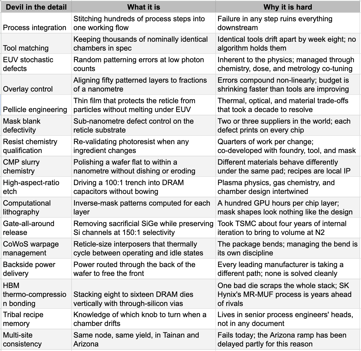
The above list is a small sample collection of the things that go into making a successful fab operation. In fact, what goes into making a cutting-edge fab is as describable as writing an essay on what makes a great artist with common pestles in her hand. It is the art part that makes TSMC wield its pricing power against everyone around it, including the supposed 100% market-share supplier like ASML.
However, there is another point out here, particularly in light of the high-sounding plans of some of the newer players from around the globe.
ASML has New Clients, or Does It?
Regardless of what we say above, there is a rising horde of entities that want to embark on building semiconductor manufacturing facilities, including some at the most advanced end. We may try to claim that the cutting edge is impossible for anyone without experience, but not everyone believes in it. Elon Musk is certainly one of them. Everything about Terafab defies conventional logic. The initial budget is massive, but plausible at around USD25bn. While the project will have Intel as a partner, one must remember the lack of experience and no working chip team. The target of a terawatt of compute requires over 20m Rubin-class wafers and over 15m HBM4E wafers, apart from a lot of other things. At realistic yields and cycle times, that is more than the capacity of a few hundred of the best current fabs. The spread between announcement and physics is two orders of magnitude.
A more grounded, yet incredibly risky, plan is unfolding in Japan. Rapidus, founded in 2022, has backing from eight Japanese conglomerates and the government, as well as technology transferred from IBM. Cumulative public funding has reached roughly USD 15 billion. Mass production is targeted for 2027, starting at 6,000 wafers per month and scaling to 30,000 later. For comparison, TSMC produces over 150,000 at leading nodes. There is no way to say whether Rapidus will succeed in these goals, but some experts see the possibility of competitive operations in single digits even by 2030.
China is the third experiment, the forced one. Sanctions block EUV. SMIC has nonetheless built a 7nm-class node using DUV multi-patterning, and Huawei's Kirin 9030 sits between 7nm and 5nm. The engineering is genuine. So is the cost. SMIC's 7nm yield is estimated at 20-40% against TSMC's ~80% at the same node. The 5nm-class yield is reportedly under 20%. Per-chip cost runs roughly 50% above TSMC's EUV-based equivalent.
The pattern across three live experiments is the same, supplemented by a half a dozen other announcements from Saudi Arabia, India, to Germany and other places in Europe. Money buys the equipment, and possibly the people. What it cannot buy is the experience that is critical in mastering the tiny steps. The instruments are sold from a catalog. The art is not.
The Apple Paradigm: The Danger of Weaponized Leverage
The cleanest way to test the "money plus engineering equals fab" thesis is to walk through the graveyard of those who tried. The list of entities that failed to crack the leading edge of semiconductor manufacturing reads like a tech hall of fame: IBM, Motorola, Texas Instruments, and a litany of once-dominant Japanese conglomerates. None of these titans lacked capital. None lacked brilliant engineers. Each had access to the exact same equipment catalog as TSMC, often years earlier. What they lacked was the institutional art. Money buys the instruments; it does not buy the instinct.
This is precisely why ASML cannot simply replace TSMC with a syndicate of ambitious upstarts. On paper, ASML holds all the cards. They possess a 100% absolute monopoly on the EUV lithography machines required to keep the AI revolution breathing. But a monopoly is only as powerful as its buyer's capacity to consume.
TSMC is not just a customer; it is a monopsony of competence. It is the only entity on earth capable of absorbing ASML's bleeding-edge supply at the volume required to fund ASML's massive R&D pipelines. If TSMC pauses its CapEx, ASML’s forward revenue projections crater. TSMC's pricing power isn’t merely derived from being the biggest; it comes from being the only player who knows how to wield the world's most expensive paintbrush without ruining the canvas.
So when TSMC walks into an industry symposium and publicly balks at ASML's staggering $350 million price tag, it is running a playbook it learned from the other side of the table. For the better part of a decade, Apple did to TSMC exactly what TSMC is now attempting to do to ASML.
Apple was its apex customer. It was effectively the only client with the sheer volume necessary to justify the financial risk of TSMC’s each new node for best part of last two decades. Apple weaponized that leverage, extracting preferential pricing and exclusive first-run access that no other customer could match. TSMC accepted the squeeze because Apple's commitment bankrolled their process leadership. But while TSMC fueled Apple’s multi-trillion-dollar ascent, its own profit margins were kept on a tight, Cupertino-controlled leash.
By now, the tables have turned. Buoyed by the insatiable demands of Nvidia, AMD, and the broader compute ecosystem, TSMC’s customer base has broadened. They no longer rely exclusively on Apple to keep the lights on. Consequently, the era of absolute preferential treatment has also ended. Today, TSMC dictates pricing and timeline terms to the iPhone maker without hesitation, forcing even Apple to wait in line.
The Warning for 2026: The Fracturing Dependency
This history reveals the long-term peril of TSMC’s current standoff with ASML. TSMC is aggressively flexing its monopsony muscles, betting that it remains irreplaceable.
But ASML’s customer base is broadening in the exact same way TSMC’s did. The dependency is fracturing. Memory manufacturers are now voracious consumers of EUV systems. SK Hynix aggressively procured roughly thirty EUV machines in early 2026, willingly paying a premium for expedited delivery, while Samsung accelerates its own EUV purchases for 1c DRAM. Meanwhile, Intel, desperate to claw back foundry leadership, has already committed entirely to High-NA for its 14A node.
The reality in 2026 is stark: the customer refusing to pay the premium for High-NA EUV is exactly one. Everyone else is buying. ASML didn't necessarily engineer this independence; the market's broadening demand for compute is doing it for them. TSMC's leverage is real but could be peaking, and they must tread carefully. In the semiconductor industry, it is remarkably wise not to do unto your suppliers what you wished your greatest customer had not done unto you.
Part Two: The Necessary Question
Equipment is not enough. That is settled. The harder question is whether ASML's latest equipment is necessary, or whether the industry can keep extracting performance from older tools and clever process work for long enough to call ASML's bluff.
The Art of Squeezing more out of the Same
When TSMC took the stage in April 2026 and declared it would stick with its current generation of Extreme Ultraviolet (EUV) lithography through at least 2029, the industry gasped. Stripped of corporate theater, TSMC’s claim was a profound flex of engineering arrogance: they believe they can indefinitely find throughput, defect, and design-rule improvements without writing a €350 million check for ASML’s bleeding-edge High-NA tools.
And as an engineering matter, they are largely right. The quietest, most consequential story of the past five years has not been the invention of new machines, but the ruthless extraction of performance from existing ones.
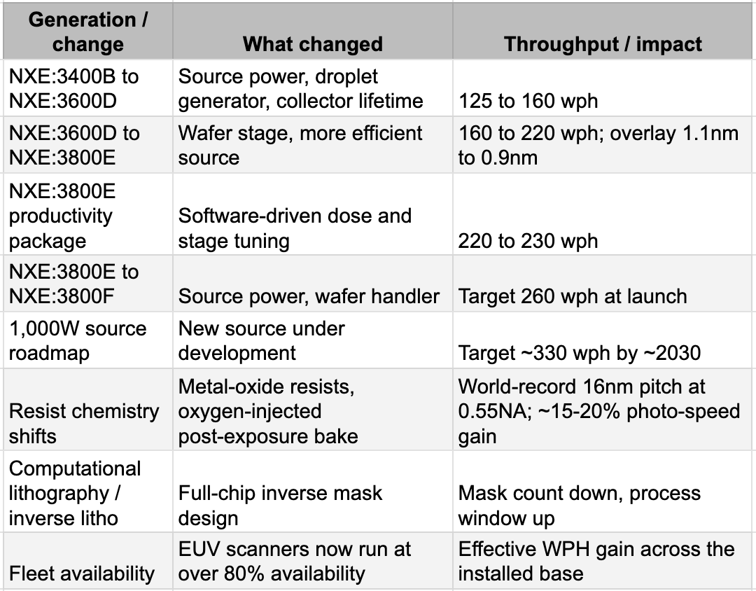
The argument adds up to something. A leading-edge logic node circa 2026 is using a roughly twenty-twenty vintage EUV scanner running at twice the productivity, with better resists, better masks, better software, and a process flow that has been reorganised around what the existing tool can do well. None of this is free, and none of this is finished. But it does mean that the question "do we need High-NA in 2027" has a credible answer of no. TSMC believes the extension runs to A14 in 2028 and possibly to A13 in 2029 without crossing into High-NA. Others may disagree on timing, but no one in the industry argues the extension is fictional.
China takes the Same Playbook to its Limit
China is running the same extension play, except without EUV at all. The result is the most strenuous test in the industry of how far cleverness can substitute for the latest tool.
Sanctions block ASML EUV exports to mainland China and have done since 2019. SMIC has nonetheless built a 7nm-class node using DUV multi-patterning, with each layer requiring three or four exposures where TSMC uses one. Huawei's Kirin 9000s shipped in the Mate 60 Pro in 2023 was the first commercial proof. The Kirin 9030, announced in 2025, sits between 7nm and 5nm by TechInsights' measurement and is the most advanced chip currently producible in China. The engineering is genuine. The cost is also genuine. SMIC's 7nm yield is widely estimated at twenty to forty percent against TSMC's eighty plus at the same node. The 5nm-class yield is reportedly under twenty. Per-chip cost runs roughly fifty percent above TSMC's EUV-based equivalent. The workaround works, but it pays a tax that only sovereign demand can absorb.
The infrastructure to support a longer Chinese run without EUV is now being built. SMEE, the state-backed lithography effort, has 90nm DUV in production and a 28nm immersion system in late development. Shanghai Yuliangsheng, linked to Huawei's SiCarrier, delivered an immersion DUV tool to SMIC for testing in September 2025. SiCarrier debuted more than thirty domestic process tools at SEMICON China in 2025. Domestic equipment share inside Chinese fabs rose from roughly 25% in 2024 to 35% in 2025. None of this matches ASML at the leading edge. All of it threatens ASML's position at mature nodes and also poses other worth-keeping-in-mind questions about the future.
There is even a Chinese EUV prototype. In December 2025, Huawei and SiCarrier confirmed a functional EUV light source using laser-induced discharge plasma rather than ASML's laser-produced plasma architecture. The prototype generates 13.5nm light at roughly 100 to 150 watts against ASML's 250 plus. No working chip has been produced. The most realistic forecasts put a Chinese EUV production attempt in 2028 and a competitive system in 2030. Even if these dates slip by two years, which they probably will, the long-term threat is not zero. Other extension paths exist outside China. Canon's nanoimprint lithography, the FPA-1200NZ2C launched in 2023, prints features at 14-nanometre resolution at roughly a quarter of an EUV scanner's price and a tenth of the power. It works for memory, particularly 3D NAND and certain DRAM layers, where overlay tolerances are forgiving. It does not work for leading-edge logic, where defectivity is too high and overlay too tight. Directed self-assembly, where block copolymers organise themselves into patterns at sub-EUV resolutions, has been a promising laboratory technology for fifteen years and remains a laboratory technology. Each of these is an argument against the proposition that ASML is forever. None is an argument that ASML is dispensable in 2026.
The Toll Collector's Gambit
But there is a fatal flaw in the extraction thesis. Squeezing more life out of current machines is a brilliant strategy, but none of it is free. And the entity collecting the toll is still ASML.
TSMC’s narrative implies a break from ASML’s pricing power, but the reality is an inescapable tether. Extending the current generation of EUV scanners is not a solo endeavor; it requires deep, continuous, and highly expensive collaboration with the manufacturer. When TSMC upgrades an NXE:3800E scanner from 220 to 230 wafers per hour, ASML doesn't send a technician with a wrench. ASML sends a software key. That upgrade is sold as a premium productivity package. The new resists require multi-year qualification loops with ASML. The replacement parts, the laser maintenance, the optics calibration—it is a closed ecosystem. The cumulative effect is that a 2020-vintage EUV tool, fully upgraded, runs roughly twice as productively in 2026 as it did at delivery, but ASML has monetized every single step of that evolution.
For decades, ASML operated like a bespoke European R&D lab that happened to sell machines. In 2026, they have finally realized they are an absolute monopoly, and they are learning to wield the pricing power that comes with it, perhaps like memory makers in 2026. If TSMC refuses to buy the €350 million High-NA tool, ASML does not starve. They simply tighten the screws on the installed base. They control the service contracts and the software upgrades for the standard EUV machines TSMC desperately needs to execute its "extraction" strategy. ASML owns the air supply.
The deeper point is that ASML's pricing power is not limited to High-NA. ASML is also the sole-source supplier of Low-NA EUV, and the dominant supplier of advanced DUV immersion. Nikon and Canon are present in DUV but irrelevant at the leading edge of immersion. The same monopoly that lets ASML price High-NA at EUR 350 million applies, in slightly diluted form, to the Low-NA tools every fab in the world is currently running and will continue to run for the next decade. ASML has held DUV pricing roughly flat through 2024 to 2026, which is a choice, not a constraint. If ASML decides to raise DUV prices materially in 2027 or 2028, the customers' realistic responses are limited.
Furthermore, the physics of extraction has a hard, mathematically brutal limit. As feature sizes drop into the angstrom era, stochastic defects, or random errors caused by the unpredictable behavior of individual photons, multiply exponentially. Multi-patterning on standard EUV requires running the same fragile wafer through the scanner two, three, or four times. Below the A14 generation, the layer count, the mask count, and the sheer cycle time of multi-patterned standard EUV start to shatter the economic viability of the node. You end up spending more money trying to force the old machine to work than you would have spent simply buying the new one.
The rest of the industry has already done this math. The memory makers concluded that the line crosses even earlier for DRAM than it does for logic. SK Hynix installed its first High-NA EUV tool in late 2025 to secure dominance in 1c DRAM and HBM. Samsung is aggressively integrating High-NA into its 2nm logic survival plan. Intel, fighting for its foundry life, has committed entirely to High-NA for its 14A node. Once again, the customer holding out at €350 million is, as of April 2026, exactly one
Conclusion: The Expiration of Politeness
For fourteen years, ASML has held an absolute monopoly on the most strategically critical machine in the global economy, yet it has wielded that power with baffling restraint. By any standard metric, they have operated more like a distinguished European research syndicate than a capitalist apex predator. Their pricing tracks engineering costs rather than desperate scarcity, and their CFO frames supplier negotiations as "healthy peer pressure." But this politeness has an expiration date. Every employee in Veldhoven must be watching the boardrooms at its Taiwanese and Korean clients gloat over absurd, historic margins. ASML must learn how to ask for more like the employees of these companies. These downstream giants wield immense pricing power and are forced into massive capital expenditures to stretch their roadmaps. As the singular physical chokepoint of the entire silicon revolution, ASML should, by every law of monopoly economics, be extracting a vastly larger tax.
The complication is that ASML does not sell across a counter to a fragmented market; it sits across a bespoke table from three or four sovereign corporate states. This extreme buyer concentration is the only reason ASML’s dominance has historically felt like a partnership rather than an extortion racket. TSMC has aggressively weaponized this dynamic, publicly drawing a line in the sand by deferring High-NA EUV until 2029. And, TSMC’s threat is now colliding with ASML's bulletproof ledger. Backed by SK Hynix placing its largest EUV order in history and a €38 billion order book, ASML can mathematically afford to let TSMC sit out the High-NA generation and still coast into a record-breaking decade.
Everything we have mapped out is theoretical leverage, but high-stakes negotiations ultimately boil down to a single behavioral variable: who blinks first. Will the next price list for standard Low-NA tools surge the way it mathematically could? Will the next software productivity package be priced like an incremental upgrade, or like the ransom-ware of enterprise tech? History suggests we should temper our expectations. The 2012 customer co-investment fundamentally wired ASML to view these giants as partners, led by a CEO who publicly refuses to be a "bottleneck." ASML’s politeness is also reflected in how it is never seen lobbying for China business the way someone like NVIDIA does. It may not succeed, but it does not even try.
So the conclusion is brutally simple. ASML holds every single card required to win this hand; the only question is whether they have finally learned how to play them.